Research highlight
Gold and glue for seamless 3D integration
‘Photonic devices need electronics for driving and control. Over the past four years, I have developed methods to merge the two into a single chip with a scalable fabrication method, without compromising their performance.’ This is how Salim Abdi summarizes the work he did as a PhD researcher in the Photonic Integration group. He successfully defended his thesis on 4 June 2025.
‘When I started here in Eindhoven, I did not have a lot of knowledge about integrated photonics,’ researcher Salim Abdi states. ‘I had obtained my master’s in physics with a focus on materials science and nanomaterials. When I discovered integrated photonics, I became intrigued by its potential in research and applications. That is why I came here to pursue my PhD in this field. After obtaining my PhD, I decided to stay on as a postdoc. Now I am working on a PhotonDelta project that aims to continue along the same path by developing photodetectors with shorter response times than those that are currently available.’
Glueing wafers
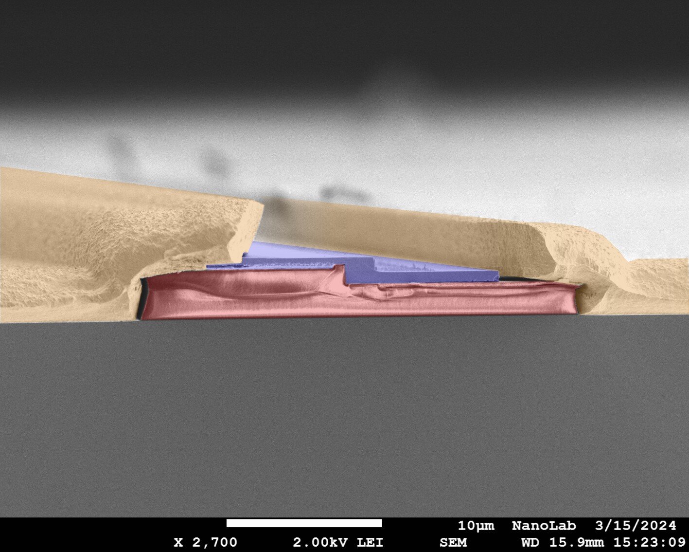
The aim of Abdi’s work is to fuse photonic devices and electronic circuits in a non-conventional manner. Usually, the two are placed side by side in a package. They are then interconnected with long gold wires, which waste power and degrade the communication speed of the final product. Abdi’s approach benefits from the third dimension, and focuses on placing photonics directly on top of electronics, leaving only a few microns of distance between the two for very short interconnects. ‘What’s unique in our approach is its large production capacity. We are doing this at the scale of entire wafers during the production process, and not for single chips individually. Here, we first glue the two wafers together, then we make connections for all photonic and electronics within the wafers through a single step that only takes seconds’, he explains.
In his PhD research, Abdi worked with indium phosphide wafers, a material known for enabling very fast photonics and electronics. ‘Even though both components are made of the same material, they are not identical. Photonics and electronic devices differ in size, layer compositions, and are manufactured in vastly different ways. That is also why it is difficult to ensure a strong, uniform, and defect-free bond between the two’, he stresses.
To solve this, the Algerian engineer investigated the use of a special glue-like material called BCB (benzocyclobutene). ‘Using BCB for bonding is simple and does not compromise the fabrication processes or the performance of the electronics nor of the photonics devices. And the beautiful thing is that the bonding technique is agnostic to whichever material platform used for either chip as well.’
Using BCB for bonding is simple and does not compromise the fabrication processes or the performance of the electronics nor of the photonics devices. And the beautiful thing is that the bonding technique is agnostic to whichever material platform used for either chip as well.
Shifting stroopwafels
BCB is fairly easy to apply, the scientist says. ‘Since the polymer turns into a liquid when heated, we can spin coat it on, and it automatically fills all the voids between the two wafers during bonding.’ Alas, there is also a drawback to this flowing behavior, Abdi adds: ‘Like what happens in a stroopwafel when the caramel between the two sides of the waffle is still hot while pressing, also in our system reflow of the liquid BCB causes the wafers to shift with respect to each other.’ And that results in misalignments of the electronic and photonic components, which can potentially undermine the fabrication process. Abdi managed to circumvent this unwanted misalignment by introducing hard BCB micro-pillars that act as anchors during bonding.
A second challenge the now postdoc managed to overcome was related to thermal management. ‘In most stacked heterogeneous devices, the photonics are separated from the substrate that is actively cooled by the bonding layer, and the latter is a bad conductor of heat,’ he explains. ‘So, if the bonding layer is too thick, the heat from the photonic devices on top cannot be efficiently released.’ This is problematic, as it degrades the performance of the device. ‘I created thick gold connections between the device and the substrate to ensure a good route for heat to be removed, hence boosting the device performance and ensuring it can be used in 3D integration.’
What’s unique in our approach is its large production capacity. We are doing this at the scale of entire wafers during the production process, and not for single chips individually
Salim Abdi | PhD
Focusing light with invisible patterns
Lasers in the sky for high-speed internet
Gold and glue for seamless 3D integration