Coming full circle in chip technology
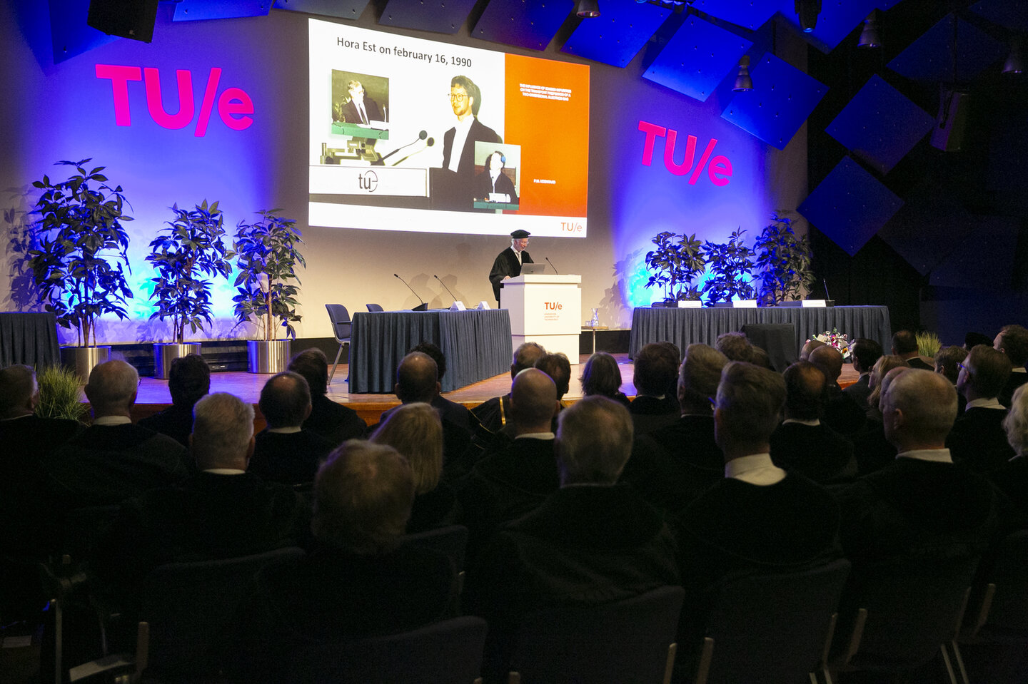
It was a visit to IBM Research that shaped the scientific career of Paul Koenraad. After having spent 39 years at TU Eindhoven, the Professor of Semiconductor Nanophysics recently delivered his valedictory lecture. ‘Finally, I have time to complete my collection of historic maps or visit cave paintings. Who knows, I might even enrol as a student again in Astronomy.’
10
When Paul Koenraad joined TU Eindhoven in 1986 as a PhD student, the Dutch government was stimulating microelectronics much like it is now investing in chip development and photonics. ‘In the MEGA chip project , Philips and Siemens were working toward realizing a 1 megabit chip. I wanted to be involved in that exciting new development. Joachim Wolter's Semiconductor Physics group in Eindhoven had just received its first Molecular Beam Epitaxy apparatus for growing III-V materials. So, I decided to pursue my PhD here.’
After his graduation, a KNAW fellowship allowed Koenraad to visit IBM Research for a couple of months. ‘That step was crucial for my career. Working in the group of Heinrich Rohrer, who a few years before my stay was awarded the Nobel Prize in Physics for his invention, I was introduced to the Scanning Tunneling Microscope.’

"We acknowledge that the transition towards quantum secure networks has to be a gradual one"
Idelfonso Tafur Monroy | Founding father of this testbed
Visualizing individual impurities
Koenraad was immediately intrigued by the possibilities this new microscopy technique offered to study semiconductor materials and structures. ‘We for example showed that cross-sectional STM could visualize individual doping atoms in semiconductors. That resulted in an article in Physical Review Letters, which opened the door to a grant to build my own STM.’
During his scientific career, Koenraad pursued two main lines of research: visualizing the growth of semiconductor structures and studying doping atoms. ‘Together with Michael Flatté I wrote a well-cited review article in Nature Materials about how you can create and manipulate a device where the functionality is based on a single doping atom, for instance in single-photon sources.’
"In the MEGA chip project , Philips and Siemens were working toward realizing a 1 megabit chip. I wanted to be involved in that exciting new development."
Paul Koenraad | Full Professor, Dean of the Graduate School
Evolution
Over the years, Koenraad has seen both the field and the group evolve. ‘We went from studying the properties of two-dimensional electron gases to directly manipulating material properties by growing nanowires and designing dielectric nanostructures. And now, researchers like Erik Bakkers are even able to convert materials from having an indirect to a direct bandgap. The partnership model, which I introduced during my time as a group leader by appointing Andrea Fiore as an additional full professor, has helped the group grow to where it is today: including multiple principal investigators who together take on big challenges, secure large investments and provide education in a wide range of related topics.’ And so, he leaves the Photonics and Semiconductor Nanophysics group knowing that it is – once again – at the center of the latest revolution of chip technology.
"We acknowledge that the transition towards quantum secure networks has to be a gradual one"