Research highlight
INSPIRE: Combining the best of two worlds
Revolutionize the production of photonic integrated circuit technology. That is the ambitious aim of INSPIRE, the five million euros Horizon 2020 project that recently started in the Photonic Integration group. The researchers will combine energy-efficient indium phosphide (InP) circuits with large-scale silicon nitride (SiN) photonic-based circuits using wafer-scale micro-transfer printing processes.
TU/e researcher Yuqing Jiao is one of the lead scientists in this project. ‘Together with imec in Belgium, TU/e is the core initiator of this ambitious project,’ he says. ‘In fact, this whole endeavor started during the first outbreak of COVID-19. We managed to establish a varied consortium consisting of TU/e, imec, Thales, the University of Cambridge, X-Celeprint, SMART Photonics, and Amires. But until this day, we have never met in person for the project.’
The aim of the project is to combine the well-known photonic materials silicon nitride and indium phosphide in a hybrid way to add their pros and cancel out their cons, says Jiao. ‘Indium phosphide has the highest efficiency in generating light at telecom wavelengths. Silicon nitride is well suited for low-loss optical waveguiding. By combining the two material systems, we will achieve a system with performance beyond what a single material system can offer.’
Scale up
The idea of transfer printing is not new. Other people have combined the two materials at a single-chip level. Imec itself has already transferred InP onto silicon with a microprinting technique. ‘We want to bring this to a higher maturity level. The current demonstrations were highly academic and at the single device level.’ In this project, the researchers explicitly aim for a reproducible process that can be scaled up to industrially relevant quantities with guaranteed quality.
The consortium harbors all necessary partners to achieve this goal, Jiao says. ‘Every partner brings in its own expertise. At TU/e, we are world-leading in indium phosphide and we have a track record in generic integration. Imec holds a similar position when it comes to silicon and silicon nitride. To connect the two, we make use of a dedicated microprinting technique developed by our partner X-Celeprint. And with SMART Photonics we have a professional indium phosphide foundry on board to help bring this technology from the lab to a higher Technology Readiness Level.’
Scientific challenges
The most important scientific challenge is in exploring the boundaries of technology. How many InP devices can be realized on top of the SiN? Will it be possible to cover the entire wafer with devices of identical quality? Which new designs can be realized? And what kinds of new applications will this combination of materials enable? ‘An additional challenge rises when the two materials are put together. Now that the InP devices are placed on top of the SiN circuits, instead of their original substrate, the generated heat in the InP devices will be harder to dissipate. Therefore, research on thermally stable InP devices, both at the material level and device design level are essential.’
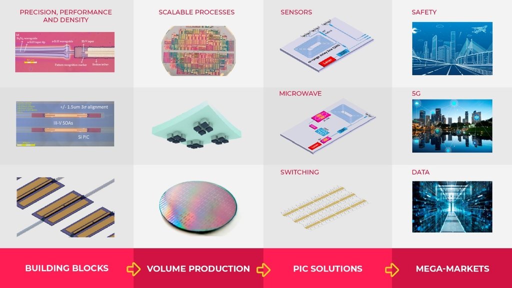
Within the project, three dedicated use cases will be explored:
- a distributed fiber sensing readout unit suited for predictive maintenance in civil engineering and transportation
- a microwave photonics radio-frequency pulse generator
- an optical switch fabric to reduce the energy consumption of data centers.’
Each of these use cases presents us with different conditions to be met,’ Jiao says. ‘Take the case of the fiber sensing. There the required linewidth of the laser and the sensitivity of the readout sensor are of great importance but quite challenging. And for the datacenter switch, we need to come up with solutions that can enable tens of channels working in parallel with hundreds of devices to be controlled at the same time.’
You can think of printing photonics on electronics, or combining photonics and MEMS platforms. I am convinced that we are working on something with an enormous potential that will become a game-changer in the communication and sensing technologies.’
Yuqing Jiao | Assistant Professor
Fabrication first
At TU/e, four researchers are involved in the project. Recently appointed PhD-student Yihui Wei will focus on fabrication aspects first, she says. ‘We will start from the proven technology and designs. As soon as we have produced the first hybrid wafers, I will verify their performance by performing electrical and optical measurements. Based on that we can start building larger circuits and explore novel applications.’ Jiao: ‘With this transfer printing technology we will be able to optimize the materials individually for each specific functionality. This provides us with additional freedom to design complex circuits and break records in terms of efficiency, power consumption, and data throughput.’
‘This project goes beyond combining indium phosphide and silicon nitride,’ Jiao stresses. ‘We want to use this as a pilot to demonstrate the power of hybrid technology and transfer printing since this idea could work with many other types of different material systems. You can think of printing photonics on electronics, or combining photonics and MEMS platforms. I am convinced that we are working on something with an enormous potential that will become a game-changer in the communication and sensing technologies.’
More information: www.inspire-h2020.eu