4
Talent
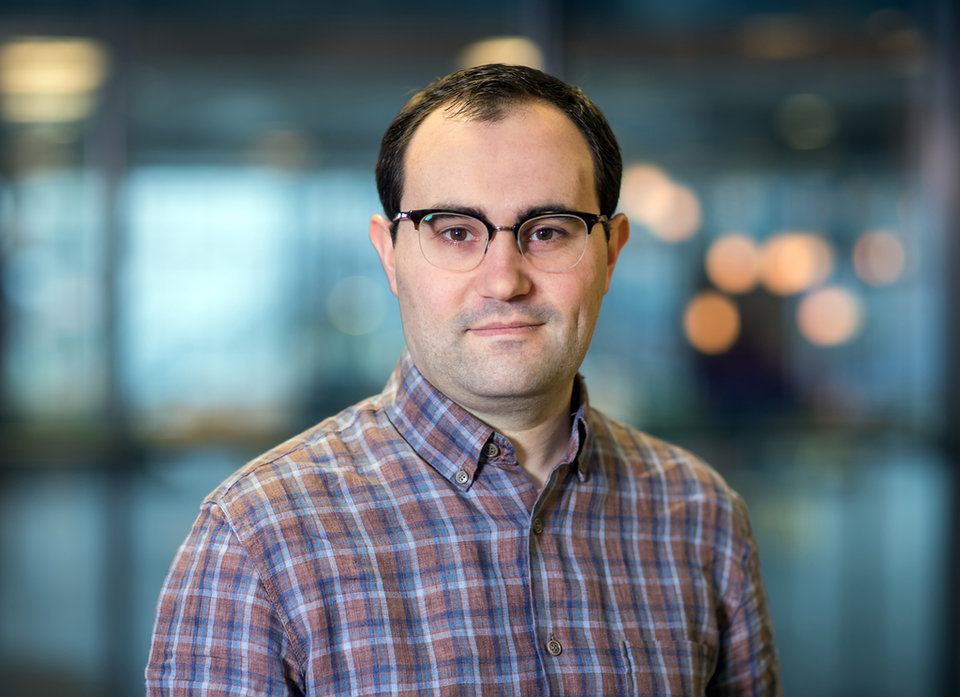
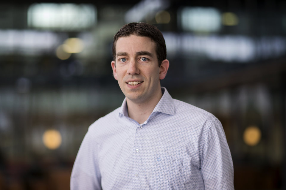
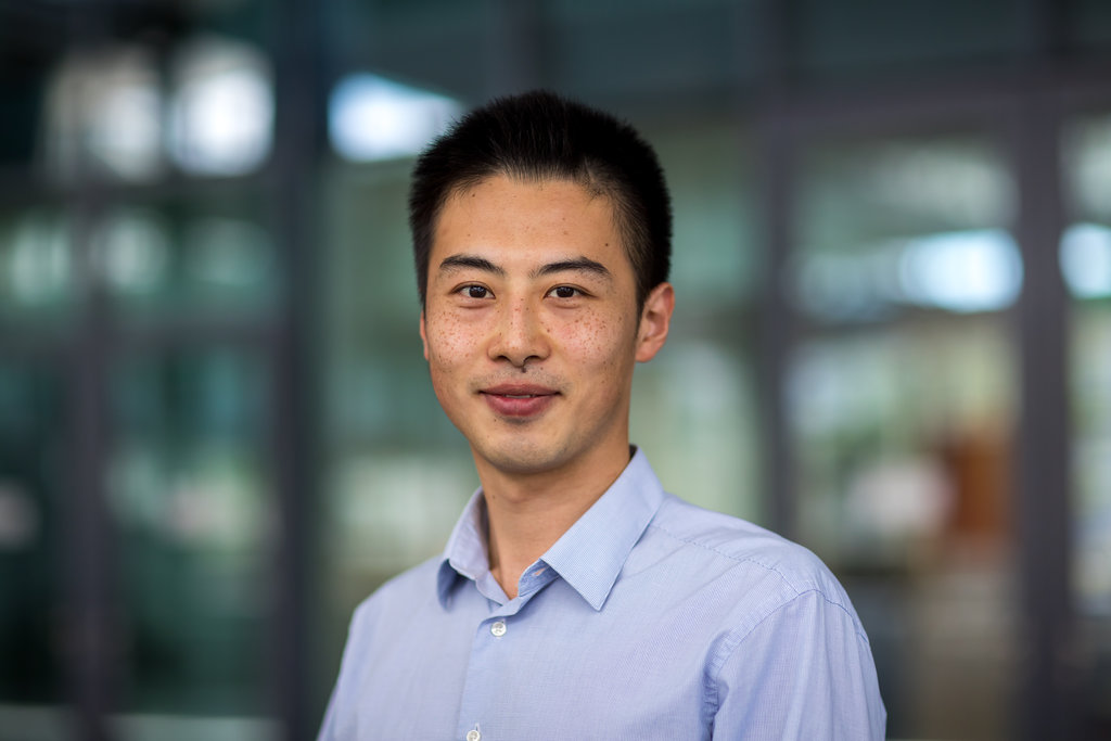
Meet Alberto Curto, Adrie Mackus and Weiming Yao.
Alberto Curto
Assistant Professor
Assistant Professor Alberto Curto is aiming to design new semiconductor nanophotonics techniques that can accurately measure the chirality of molecules. ‘Most biological molecules have either right- or left-handed conformations,’ Curto explains. ‘This so-called chirality plays an important role in the interaction between pharmaceuticals and the human body, for example.’ Sometimes one of the enantiomers is an efficient remedy for a certain disease, whereas its mirror image might not work or even be harmful. ‘Also for other applications, chirality is of importance,’ Curto adds. ‘For example, in the food industry taste and fragrance depend on molecular enantiomers.’
Read more
One floor above Alberto Curto in the Flux building, second ERC grantee Adrie Mackus is also hiring. He is looking for people with backgrounds in physics, chemistry, experiments and simulations to help him develop a new method to build nanostructured materials from the bottom up. ‘Traditionally, nanopatterns, like for instance for electronic or photonic chips, are made by a top-down process,’ he explains. A layer of material is grown, with the aid of a high tech kind of light projector a pattern is imaged on top, and subsequently all of the material outside of that pattern is etched away.
Read more
Adrie Mackus
Assistant Professor
Weiming Yao
Assistant Professor
Weiming Yao, assistant professor in the Photonic Integration group and recipient of a NWO Veni grant, has been captivated by the possibilities of integrated photonics since his bachelor studies in Electrical Engineering. After having studied in Germany, the UK, Italy and Japan, he decided to settle at TU/e to explore the potential of this technology.
‘Some of my colleagues and lecturers had experiences with TU/e and talked highly of the research here. After I obtained my master’s degree, I applied for a PhD position. Subsequently, I got the opportunity to be involved in a new Photonic Integration Technology Centre initiative.
Read more

“With our experience in developing dielectric optical antennas, ours is the perfect group to design nanophotonic resonators to enhance chiral light-matter interactions.”
Alberto Curto
Assistant Professor Alberto Curto is aiming to design new semiconductor nanophotonics techniques that can accurately measure the chirality of molecules. ‘Most biological molecules have either right- or left-handed conformations,’ Curto explains. ‘This so-called chirality plays an important role in the interaction between pharmaceuticals and the human body, for example.’ Sometimes one of the enantiomers is an efficient remedy for a certain disease, whereas its mirror image might not work or even be harmful. ‘Also for other applications, chirality is of importance,’ Curto adds. ‘For example, in the food industry taste and fragrance depend on molecular enantiomers.’
Trace a single chiral molecule
Curto’s ambitious target is to develop a system that is able to map with nanoscale spatial resolution the chirality of the lowest possible molecular concentrations down to a single chiral molecule. ‘The current methods to identify the handedness of molecules use circular dichroism, which measures how light of different polarizations is absorbed by the molecules. Unfortunately, these methods lose their sensitivity at low concentrations, while for medical purposes, it would be very interesting to map where a chiral drug is getting inside the cell, whether or not its chirality is preserved, and how that relates to its efficacy.’
Two routes
In his research, Curto makes use of his broad expertise in enhancing the interaction between materials and light. ‘With our experience in developing dielectric optical antennas, this is the perfect group to design nanophotonic resonators to enhance chiral light-matter interactions.’ The project proposes two routes to achieve this. The first idea is to design nanophotonic structures with fine control of electric and magnetic dipole resonance. ‘Our challenge is to find the right geometry for optimal circular dichroism response, which according to theory might even be higher than that of a plane wave in free space.’
The second route, which is of a more fundamental nature, Curto says, explores the possibilities of so called excitonic sensors based on atomically thin semiconductors. ‘We are looking at graphene-like two-dimensional structures, produced by exfoliation from bulk material. We work with two dimensional semiconductors with a high quantum efficiency and a strong spin-valley polarization. Here we want to exploit the interplay of photons, charges, and spins.’
Finding the right people
Within this project, developing the instrument will be the main challenge, Curto says. ‘We want to measure very small changes in polarization with high resolution, so we will need to create new equipment.’ But the determining factor for success lies in finding the right people, he emphasizes. ‘So if you have an optics background in applied physics, electrical engineering, or physical chemistry, and you are fascinated by light, please contact me to discuss the possibilities!’

“We now want to make the step to area-selective ALD, which enables us to grow the material only where it is needed.”
Adrie Mackus
One floor above Alberto Curto in the Flux building, second ERC grantee Adrie Mackus is also hiring. He is looking for people with backgrounds in physics, chemistry, experiments and simulations to help him develop a new method to build nanostructured materials from the bottom up. ‘Traditionally, nanopatterns, like for instance for electronic or photonic chips, are made by a top-down process,’ he explains. A layer of material is grown, with the aid of a high-tech kind of light projector a pattern is imaged on top, and subsequently all of the material outside of that pattern is etched away. ‘That approach starts to have some disadvantages when you want to build ever smaller, ever more complex three-dimensional structures, like in photonic or electronic chips for quantum computing.’
With his ERC Starting Grant, Mackus aims to develop new approaches for so called area-selective atomic layer deposition (ALD), a technique that grants its user atomic-scale control. ALD allows for the deposition of thin films of materials on a substrate, by exposing the surface to alternating precursors in a vapor phase. The precursor molecules react with the surface in a self-limiting way, stopping the reaction once all the reactive sites on the substrate have been used.
Start from known technologies
'We now want to make the step to area selective ALD, which enables us to grow the material only where it is needed. That would eliminate a lithography step and the associated alignment error between the different layers of material,’ Mackus says. ‘The research explicitly starts from techniques that are known in industry’, he emphasizes. ‘Other groups working on area-selective ALD often make use of self-assembly processes, but these are not sufficiently reliable and too time-consuming to be of any interest for industry. We start from known technologies in industry, and try to combine and further develop them in such a way that they become scalable alternatives for lithography.'
Combined strength of chemistry and physics
Mackus is going to combine a chemical technique, using specialized, small organic inhibitor molecules, with a physical technique, using plasmas to control the direction of growth. ‘A standard ALD process uses two different chemicals. We are adding an extra step of organic surface molecules that block deposition on the areas where you don’t want to write any structures. On top of that, we use plasmas to direct the deposition. Where we would normally only grow layers on for example the dielectric material and not on the metals, we can now also grow only on either the horizontally or vertically-oriented surfaces.’
While the first focus of his project is on nanoelectronics, Mackus also keeps an eye on applications in photonics, he says. ‘Since photonic chips also consist of 3-dimensional nanostructures that need to be fabricated with accurate control, I see ample potential of this technique for photonics as well.’

“Photonics has the potential to overcome problems associated with complex networks of artificial neurons.”
Weiming Yao
Weiming Yao, assistant professor in the Photonic Integration group (and recipient of a NWO Veni grant), has been captivated by the possibilities of integrated photonics since his bachelor studies in Electrical Engineering. After having studied in Germany, the UK, Italy and Japan, he decided to settle at TU/e to explore the potential of this technology.
‘Some of my colleagues and lecturers had experiences with TU/e and talked highly of the research here. After I obtained my master’s degree, I applied for a PhD position. Subsequently, I got the opportunity to be involved in a new initiative, the Photonic Integration Technology Center. I was intrigued by the opportunity to work on more application-oriented projects, since I wanted to see a direct impact of our research outcome.
After three years of technology development, I decided it would be nice to return to basic research again, as both aspects need to go hand in hand for technology to advance. Recently I have been awarded a Veni grant to explore and realize artificial neurons in integrated photonics, in order to develop faster and more efficient AI hardware. When networks of artificial neurons get more complex, electronic hardware has some disadvantages, like extensive heat dissipation or electrical parasitics, leading to limitations in power efficiency and speed. Also, the Von Neumann architecture, which is the standard architecture for computers these days, is not the most convenient for performing artificial neural network computations in parallel. In this architecture, information needs to travel back and forth from memory to processing unit, which is a bottleneck. Photonics has the potential to overcome these problems. Another advantage is that with a laser, it is easy to emit short pulses, which is ideal for simulating spiking signals that resemble the spiking neurons in the human brain. In electronics, this is too cost ineffective, and way too slow.’
Scaling up
‘The big challenge is to scale up from one photonic neuron towards entire networks. Since you are working with multiple cascaded lasers and optical components, you have to deal with interference effects and unwanted reflections, leading to instabilities.
The Veni project has two main goals. First, we want to understand and exploit the dynamics of lasers to demonstrate a spiking optical neuron. Then we want to go from one neuron to a small network of neurons and explore its scalability constraints.
In my research, I am actively collaborating with colleagues from the Electro-Optical Communications group, especially with Patty Stabile, who is working on neuromorphic photonics from a system perspective. We discuss ideas and hope we can fit my spiking neurons into her photonic networks. I find it fascinating that integrated photonics is a technology which arose from a few specific applications but starts to gain a much bigger scope today, showing great potential for realizing photonic neurons in my case. I strongly believe that photonics can become a useful tool to accelerate complex AI computations. Since optical neurons bear the opportunity for fast spikes and low latency, one of the ideas is that once scaled up to millions or billions of neurons, it can help advance the understanding of human cognition.’
Collaboration with industry
‘After my studies in different countries, I deliberately chose to stay in Eindhoven, since TU/e stands out for with its collaboration with industry. I haven’t seen this at a comparable scale anywhere else. TU/e research very often results in industrial impact. Spin-offs that came out of the photonics research here are already very prominent and well-known in industry. Industry integration in research programs is very strong here with frequent interactions, for example between our research institute and photonic companies at the High Tech Campus. And since my goal is to bridge fundamental research with industrial applications, this is for me the place to be.’
Weiming Yao obtained a dual MSc degree in Photonic Networks Engineering from Aston University, UK, and Scuola Superiore Sant'Anna, Italy, in 2012. His MSc thesis was on optical signal processing in fiber, performed at Osaka University, Japan. He then conducted his PhD research at TU/e, exploring high-capacity, high-density integrated optical transmitters, leading to the PhD degree summa cum laude in 2017. Since then, he has continued to work at TU/e on photonic integrated circuits as a researcher.