Research highlight
Integrated optical sensor for semiconductor metrology
In June 2020, Tianran Liu defended his thesis on ‘Controlling and sensing light on a chip using nanophotonics’. One of the findings in his thesis is an optical sensor that paves the way for an integrated sensing platform for metrology.
Adapted from the original text by Barry Fitzgerald, Science Communication Officer at TU/e
Accurate displacement and force measurements at the nanoscale are crucial for the semiconductor industry. Fully integrated and compact optical sensors including lasers and detectors in a single sensing platform could play a pivotal role here. During his PhD research at the TU/e, in the Photonics and Semiconductor Nanophysics group, Tianran Liu developed a new, integrated optical sensor that provides the resolution needed for most demanding metrology applications. His results were published in Nature Communications.
Speeding up sensing
In the age of nanoelectronics, optical read-out sensors based on optomechanical systems are frequently used in sensing applications such as in atomic force microscopes (AFMs). These devices generate sub-nanometer resolution images by measuring the laser light reflected by the deflection of a cantilever over a surface of interest. ‘In a conventional AFM, you need a laser to shine the light on the cantilever, and a photodetector to detect the reflected light,’ Liu explains. ‘Though this works rather well, only one cantilever scans the surface and the measurements are extremely slow. The ultimate aim of the research project I have been working on, is to achieve greater speeds by using multiple measurement systems in parallel. To make this possible you need very small systems and that requires having all of the equipment on a chip.’
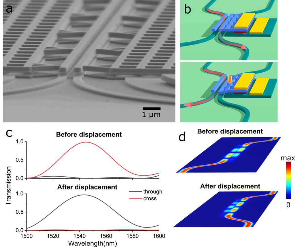
The main challenge there was to come up with the appropriate design and fabrication methods, he says. Traditional approaches use an interferometer with a moving part. These, however, tend to be large. ‘Our idea was to use a directional coupler with a movable arm as a displacement platform. That is quite different from a traditional Mach Zehnder interferometer. On top of that, it was the first time that complex MEMS structures were to be fabricated on the indium phosphide IMOS platform. So after a smooth first year of my PhD project, working out the theory, it took until the end of my third year before I got a breakthrough in the lab. And it wasn’t until the end of my PhD that it started working.’
“The ultimate aim is to achieve greater speeds by using multiple measurement systems in parallel. That requires having all of the equipment on a chip.”
Tianran Liu | Postdoc
Four waveguides
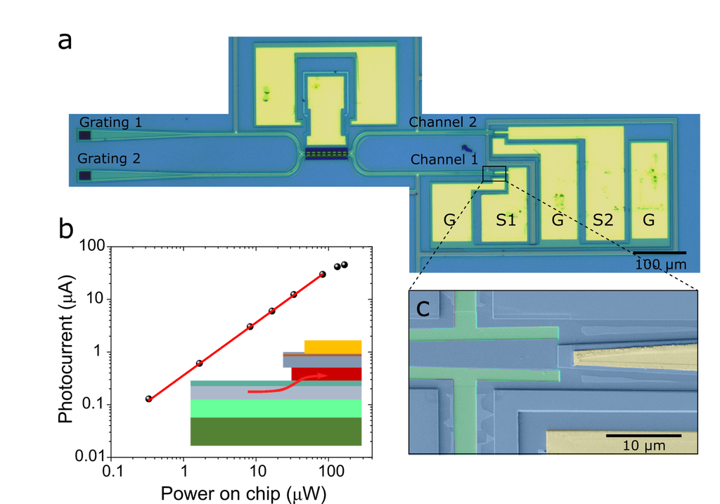
The sensor is based on the indium phosphide (InP) membrane-on-silicon (IMOS) integration platform, which is ideal for including passive components such as lasers or detectors. This platform is being developed at TU/e’s Photonic Integration group in the framework of an NWO Gravitation program and several EU projects. The sensor itself consists of two waveguides suspended above two output waveguides. When a suspended waveguide is pushed towards the output waveguides on the InP membrane, the relative amount of light carried by the output waveguides varies. Fabrication takes place via a series of lithography steps to define the waveguides and cantilever, and the final chip consists of the transducer, actuators, and photodiodes.
The new optomechanical device has a resolution of 45 femtometers in a measurement time of a fraction of a second. Crucially, the device has an ultrawide optical bandwidth of 80 nanometers. Since the sensor operates in a large range of wavelengths, the need for an expensive tunable laser for the read-out is eliminated. Liu: ‘Other efforts in displacement sensing usually require narrow band lasers that are expensive and hard to integrate on a chip. Our solution can cope with simple fixed-wavelength lasers like the ones that are currently used in AFMs.’
In terms of displacement resolution, the sensor matches the performance of traditional, bulky AFM sensing heads. Using this new device as a foundation, the researchers plan on developing an entire ‘nanometrology lab’ integrated on a chip that can be used for semiconductor metrology, and can be instrumental in pushing the limit of semiconductor technologies. The first step is to integrate a laser on the chip as well.
Intensified cooperation
‘This project has intensified the cooperation between the Photonics and Semiconductor Nanophysics group at the department of Applied Physics and the Photonic Integration group at the department of Electrical Engineering,’ Liu says. Together, both groups are continuing the work on the sensor, with the aim to fabricate a device with an integrated laser on chip. Liu himself currently holds a postdoc position in the Photonic Integration group, where he is developing an integrated sensor to measure the alignment of wafers inside a lithography machine.
More information: www.nature.com/articles/s41467-020-16269-7
Revolution: light-emitting silicon
Reprogrammable photonic integrated circuits
Integrated nanometer scale sensing