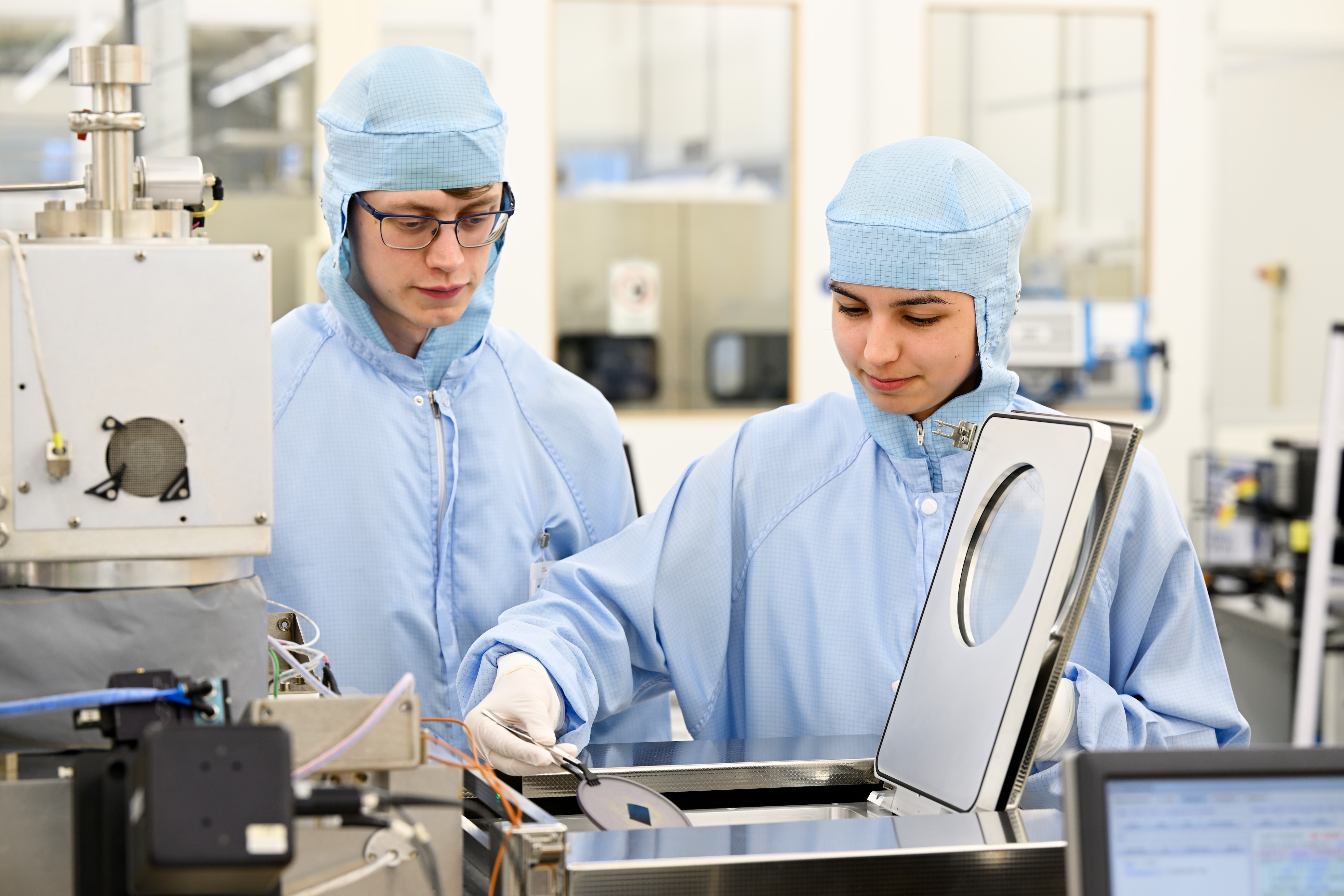
Merging photonics and electronics for future chips
To enable the revolution novel developments like artificial intelligence will bring, we need to design and manufacture chips that can generate, process and transport enormous amounts of data at extreme speeds. Integrating electronics with photonics in so-called heterogeneous chips is the way to go to meet future demands, argues Martijn Heck, Professor in Photonic Integration.
7
In spring 2024, TU/e launched its Future Chips Flagship. At the occasion, ambassador of this initiative Bart Smolders stated: ‘We are the chip university of the Netherlands. Not only when it comes to electronic circuits on chips, but we have also been active in photonic integrated chips for over 25 years.’ It is exactly this combination that holds the key to unlocking the full potential of novel developments like artificial intelligence, says Martijn Heck. ‘The development of electronics has for long been dictated by Moore’s law, which states that the number of transistors in an integrated circuit, and thus the chip’s computing power, doubles about every two years. That also means that the bandwidth for data transfer has to double in that same period of time.’
In general, electronics is used to carry out high-speed computation and generate and store data, while photonics is used to transfer these data between individual devices and data centers, through interconnects and the network. The problem is to connect the two in such a way that the ever-increasing amount of data can be generated, processed and transmitted at the right speeds, and with an energy consumption pattern that is sustainable in the long term. Heck: ‘To make this explicit: Koomey’s Law dictates that the energy consumption per compute operation goes down by 50 percent every 1.5 to 2.0 years.’

"We acknowledge that the transition towards quantum secure networks has to be a gradual one"
Idelfonso Tafur Monroy | Founding father of this testbed

"When we want to truly integrate both technologies, creating a mutual understanding is the first step. And that works best when you are actually developing something together."
Martijn Heck | Full Professor
Learn the language
Over the past years, photonics has already slowly but surely been moving closer to the electronics, says Heck, for example when it comes to electronic chips that are surrounded by optical transceivers, e.g., for datacenter switches. On the other hand, state-of-the-art optical modulators and detectors increasingly need to be closely interfaced with fast driver electronics and digital signal processing. However, to reach full heterogenous integration, where both technologies are integrated onto a single chip, we need a radically new approach and mindset, the scientist says. ‘Electronics and photonics look at similar concepts in an entirely different way. For example, when you talk about a laser, photonics people will be mainly interested in aspects like its required output power and wavelength. But for someone working in electronics, a laser is a diode, for which the main parameters of interest are the operational voltage and current.’
So, when we want to truly integrate both technologies, creating a mutual understanding is the first step. And that works best when you are actually developing something together. One example is the HiCONNECTS project, in which the TU/e groups of Photonic Integration, Electro-Optical Communication and Integrated Circuits collaborate to realize highly efficient, ultra-fast optical transmitters on an indium phosphide membrane platform, that are suitable to be heterogeneously integrated with driving electronics.
Back to the drawing board
When designing such a heterogeneously integrated system, the key is to not put the best possible electronics solution together with the optimal photonics design, but to optimize the combined technology as a whole, Heck emphasizes. ‘You need to go back to the drawing board, and start from the basic questions: what is your device supposed to do, and which design can you come up with that maximizes bandwidth, minimizes use of energy, is compatible with mature semiconductor technology nodes, and minimizes interference, crosstalk and electronic parasitic effects? A holistic view is required here.’
Impulse for future chips
In the coming years, TU/e will expand its key position in global academia in the field of semiconductors with its Future Chips Flagship. The university’s expertise on designing electronic chips, combined with its leading position in indium phosphide on silicon heterogeneous integration, makes TU/e uniquely suited to take the lead in this development. Heck: ‘Most universities do not work on heterogeneous integration, as it is a tough line of research. But these types of disruptive technological innovations usually take at least ten years, and the clock is ticking if we want to keep meeting the ever growing need for data without consuming all of the world’s available energy along the way. So, being a publicly funded research institute, I think we have an obligation to deep dive into this.’
What’s more, we need to teach new generations of engineers to look beyond the scope of electronics or photonics alone, Heck states. ‘To this end we are currently developing a new master track, which will train so-called π-shaped engineers: people who are specialized in both fields. We need people who combine in-depth knowledge of topics like chip design, integrated photonics, RF and mixed signal electronics, and digital electronics, and are able to think along multiple lines simultaneously. Because in the end, the future of both our semiconductor industry and that of integrated photonics will be a heterogeneous one. That is the only way we can meet our hunger for data in way that is sustainable towards the future.’

"We acknowledge that the transition towards quantum secure networks has to be a gradual one"