Research highlight
Paving the future with photonic membranes
Over the past couple of years, TU/e researchers have developed and demonstrated a promising novel technology called indium phosphide membrane on silicon (IMOS). Lead researchers Yuqing Jiao and Jos van der Tol talk about the current state of affairs, how the research got to this point and what is in store for the near future.
The story starts about ten years ago, Yuqing Jiao, Assistant Professor at the Photonic Integration group, recalls: ‘Scientists from the former institute COBRA had developed a platform that enabled the creation of all necessary photonic building blocks on a single chip. That platform was transferred to the SMART Photonics foundry, and for the academic researchers the question arose what had to come next.’
For inspiration, the scientists turned to the field of electronics. That is dictated by the Moore’s law, where the number of affordable transistors on a microchip has been doubling every two years. ‘For photonics, we saw a need and an opportunity for the same trend,’ Jiao comments. ‘The technology now in production at SMART Photonics is amazing. The first pure-play foundry is here in Eindhoven and provides great solutions for telecommunications, and a range of new emerging applications in sensing and metrology. But future photonic systems will need order-of-magnitude performance and functionality improvements, while consuming less energy. For futuristic domains like neuromorphic computing, we need to be able to put tens of thousands of photonic devices on a single chip, meaning that we have to significantly shrink the dimensions of the individual components, and the distances between them.’
Membranes for miniaturization
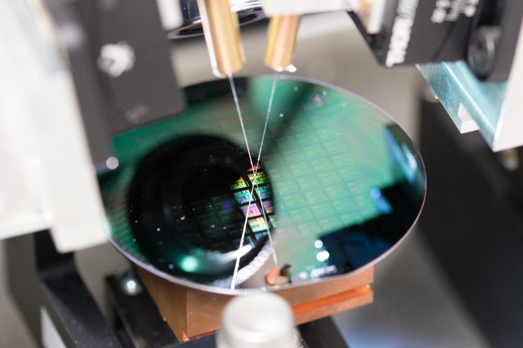
Former Associate Professor Jos van der Tol was involved in this development almost from the beginning. He recollects: ‘We came to the conclusion that we needed to revert to thin indium phosphide membranes. By using membranes, you can achieve high contrasts in refractive indices, allowing for efficient confinement of the light. Together with Ghent University, we managed to integrate a detector and a laser in indium phosphide membranes. And we even set several world records, e.g., when it comes to reducing losses in the material.’
Jiao adds: ‘We started by demonstrating a waveguide that was already five to ten times smaller than in the current commercial InP technology. Then we moved on to the platform development including the actives Jos describes. In recent years we even demonstrated membrane amplifiers and high-speed photodiodes, both integrated with the
nanophotonic waveguides. That has gained a lot of interest from outside, both from industry and from academia. They saw the potential value of this technology and started working with us.’
Yuqing Jiao | Assistant Professor
Unique approach
The uniqueness of the IMOS approach is that it integrates miniaturized waveguide circuits with light-generating actives and antennas that can communicate and interact with the outside world without the need of bulky fibers or lenses. Jiao: ‘Other platforms currently cannot offer all at the same time. At the moment, we are working on a variety of projects with end users towards specific applications.’ That doesn’t mean the science is done, he emphasizes. ‘The required miniaturization drives us to push the design and technology to higher and higher densities. This is challenging, since the smaller the structures, the stronger the interactions between light and materials. On one hand we need to significantly improve the reproducibility and control of our thin films. And a lot of effort goes into preventing the device from heating up, since that lowers its performance. On the other hand, the strong interaction enables new materials and functions into the platform, for instance non-volatile phase change materials and magneto-optic films.’
Potential applications the group is currently investigating vary from remote sensing and metrology to free space communication. Van der Tol explains: ‘Photonic technology is ideal in situations where electronics is not an option. Think of how powerful an optical sensor can be, when we can get rid of bulky lenses and enable massive parallel sensing.’
Even though nowadays, most of the current research on this topic is rather application-oriented, this technology arose from a deeply fundamental effort, Jiao emphasizes. ‘When we started this research, it was high risk, high gain. Even after the first five years we were not sure if it would be feasible at all to realize amplifiers in our membranes. This was true open-
ended research, based on a firm belief that miniaturization and increasing complexity is the future and that this is a technology worth developing. The NWO Gravitation program “Research Centre for Integrated Nanophotonics” has been instrumental in this development. And look where we are now, with multiple projects exploring a vast range of different applications together with industry and end users.’
First IMOS MPW open for applications
During the annual European Conference on Optical Communication in Basel, the joint European platform for photonic integrated components and circuits JePPIX announced that it provides broad access to the IMOS active nanophotonic research platform as a multi-project wafer service. JePPIX’s coordinator Katia Panina explains: ‘We are planning a multi-project wafer run in the first quarter of 2023 for users to benefit from this unique combination of nanophotonic integrated components. Users will be provided with a process design kit so they can design their own IMOS-based chips. This provides a feedback loop to optimize the portfolio of components for new applications. We already anticipate ten designers for the first wafers. These projects will provide proofs of concepts for leading research teams around the world, as well as a scientific validation of the platform.’
Putting the spotlight on biomolecules
Spectral sensing catches the eye
Paving the future with photonic membranes