Funding foundations for new fields
One of the main goals of the Eindhoven Hendrik Casimir Institute is to stimulate interdisciplinary research. After one year of existence, seed money was allocated to projects that represent a new combination of people and expertise. In the field of photonics, three teams of researchers received funding to work on a photonic lens for charged particles, the implementation of liquid crystals for photonic computing, and novel fabrication technologies for terahertz sensing.
3
Photonic lens
Tom Bradley from the High-Capacity Optical Transmission laboratory at the Electro-Optical Communications Group from Electrical Engineering will collaborate with Jom Luiten from the Coherence and Quantum Technology group at Applied Physics on establishing an interaction between quantum technology and photonics.
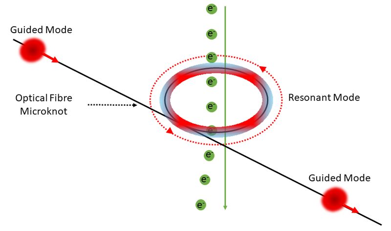
Tom explains: ‘From my previous work on fibers interacting with atomic vapors, I got the idea to use fibers for the study of light-matter interactions. When I contacted Jom, he was interested as long as that matter was in fact electrons. The idea is that, by exploiting capabilities we are developing in our lab, we taper optical fibers to reduce their diameter, thereby controlling the electric field at the fiber boundary and thus engineering a large evanescent electric field. We bring these tapered fibers into the vicinity of an electron beam to study the electron-photon interaction. The advantages of this solution are that we do not need any large lasers, no metal disturbs the e-beam, and the system can be integrated since it is compact. In fact, what we are creating is a photonic lens for charged particles, which could be of use for quantum-enhanced spectroscopy, generating entangled electron-photon pairs and with potential application in quantum communications. The fiber technology and fiber processing are ready to do the job. The challenge for this project is to work within the environment of a transmission electron microscope and to precisely position the fibers. But if we succeed, this project might be the beginning of a new
field exploiting confined micro-structured optical fiber for quantum sensing and control. We see an opportunity to seed these techniques, thereby developing technology from QuantumDelta National Growth Fund projects in Quantum computing CAT1 and Quantum Communications CAT2 into new projects for Quantum Sensors CAT3.’
Steering light waves for computing
Danqing Liu from the Stimuli-Responsive Functional Materials & Devices group at Chemical Engineering and Chemistry and Weiming Yao from the Photonic Integration group at Electrical Engineering found each other in an ambitious plan to combine polymer-based liquid crystals with photonic chips for futuristic computing applications.
Liu: ‘I make materials for robotics. Since we need electronics to drive movement, I approached Weiming to see how we could collaborate. Together, we came up with the idea to incorporate a new material into a photonic device.’ Yao: ‘My ambition is to use photonics to accelerate computation. For novel computing concepts such a neuromorphic computing, we need to move towards new architectures that allow for more parallelism. The big advantage of using optics instead of electronics, is that optics allows for different ways to achieve parallelism, for example by using different wavelengths, polarization, or modes. Our idea is to put islands of tunable polymers on top of an optical device. By changing the molecular structure of the liquid crystals, for example with light or by applying the voltage, we will be able to tune the refractive index, thus allowing for different optical modes to propagate through the device.’ Liu: ‘Though liquid crystals are a known material, for this purpose we will need to stretch their diameter by a factor of a hundred. We need to find out which mix of polymers can achieve the required range of refractive indices and how to synthesize them. And we need to find out how to process the material onto the optical device without deteriorating its performance.’ Yao: ‘From an electrical engineering perspective, the main challenges will be both in manufacturing – how can we connect electrodes to the liquid crystals – and on the theoretical side: what signal processing techniques and non-conventional algorithms do we need to perform the needed computation? Our ultimate aim with this project is to deliver a proof of concept that the combination of liquid crystals and photonic devices works to opens up a new field where we can configure elements towards computation applications.’
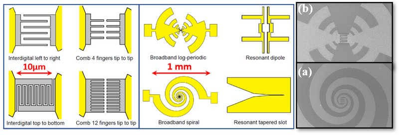
Fabricating various graphene electrode configurations, and with various antenna designs. Graphene-based THz sources and detectors with LT-GaAs (Produced in the NanoLab@TU/e. (a) Log-periodic antenna, (b) Spiral antenna.
Advanced material for highly sensitive THz devices
Shihab Al-Daffaie from the Electro-Optical Communications Group at Electrical Engineering found the NanoLab@TU/e and Jaime Gomez Rivas from the Semiconductor and Nanophysics group at Applied Physics in his ambition to produce high-quality and enhanced terahertz detectors using nanomaterials like graphene. He explains: ‘We are aiming at the maximum improvement of efficiency by novel material combinations and structures and focusing on patterned graphene in combination with molecular beam epitaxy (MBE) low-temperature growth of gallium arsenide (LT-GaAs). The development of novel processes of LT-GaAs is done by intentionally producing traps in the material. These traps enable fast recombination of electron-hole pairs. In this project, we will develop a new fabrication process to put a layer of graphene on top of this high-speed material to improve the efficiency of THz devices. When selecting the device concepts, we will limit ourselves to options that can be integrated into on-chip or on-board THz systems, opening the possibility of portable THz systems that could be deployed for remote sensing and metrology applications. This project should lead to the development of a new track at the NanoLab to grow materials for terahertz applications. The outlook is promising: we officially started on June 1st, and already have a first wafer and first devices we are currently characterizing. Since the first follow-up projects are now in the pipeline, the seed money is already starting to pay off.’