Advanced pilot line for next-generation PICs
Recently, TU/e installed the fabrication equipment of a brand new pilot line that enables the transition from 3 inch to 4 inch indium phosphide wafers for photonic chip production. Program manager Victor Calzadilla and epitaxy engineer Akanksha Kapoor explain what the pilot line consists of and what it is meant for.
3
Akanksha Kapoor and Victor Calzadilla, who led the 3-to-4 inch PIC epitaxy transition in cooperation with AIXTRON and SMART Photonics.
Victor Calzadilla | Assistant Professor
To accelerate the maturation of photonic integrated technology and to empower users to test, validate and scale up their designs for photonic integrated circuits (PICs), over the past few years, several pilot production lines have been established across Europe. One of the branches on this growing tree is transitioning InP PIC fabrication technology from 3 inch to 4 inch wafers.
One of the branches on this growing tree is transitioning InP PIC fabrication technology from 3 inch to 4 inch wafers. The pilot line consists of three consecutive manufacturing stages: TU/e’s NanoLab houses the equipment for the manufacturing of the raw indium phosphide PICs (where manufacturing itself is taken care of by SMART Photonics), optical interfacing is done at the Vrije Universiteit Brussel, and the packaging is handled at the Tyndall National Institute in Cork, Ireland. The pilot line is funded by the INTERREG project OIP4NWE and QuantumDeltaNL. More recently, PhotonDelta Growth Fund has provided additional funds to consolidate the TU/e part of the line.
‘The 4 inch pilot line is a European effort for joint technology development in InP integrated photonics’ says TU/e’s Victor Calzadilla, who is leading the OIP4NWE project. ‘This new infrastructure is meant for mid Technology Readiness Level developments, to bridge the gap between academic findings and production by commercial parties.’
“This new infrastructure is meant for mid Technology Readiness Level developments, to bridge the gap between academic findings and production by commercial parties.”
Victor Calzadilla | Leader of the OIP4NWE project
Better layers at the basis
Together with two of the project partners, pure-play foundry SMART Photonics and equipment manufacturer AIXTRON, TU/e is responsible for the front end of the pilot line, involving equipment and process development for epitaxy, deposition of dielectrics and etching of semiconductors, Calzadilla tells. One of the working horses in Eindhoven is the newest generation of epitaxy tooling, provided by AIXTRON, adds epitaxy engineer and postdoc researcher Akanksha Kapoor. ‘We use Metal Organic Chemical Vapour Deposition to build the layers of indium phosphide that our chips consist of. That means that all of the materials are in the gas phase, and deposition is driven by thermodynamics. Besides being able to handle significantly larger wafers, our new equipment also enables us to gain a more precise control over the temperature in the vessel, which is directly related to the growth properties of the layers.’
An additional feature of the new system Kapoor is very happy about, is the possibility to monitor the growth of the layers in situ. And finally, the new system is less prone to contamination, she explains. ‘The automated cassette- to-cassette wafer loading rules out the need for manual interference with the wafers. What’s more: the system features in situ cleaning options to get rid of any residual materials that might have been left behind from a previous run. So for every new deposition, it is as if you are starting with a brand new system.’
All in all, the new epitaxy machine alone will already be responsible for a huge improvement in the quality of the photonic chips that will come out of the pilot line, Kapoor is convinced. ‘A good photonic chip literally starts with good layers of material. With this machine, we will be able to produce more uniform layers, which contain less defects, and will be more uniformly doped. This will for example lead to more controlled and better emission efficiencies of the lasers we make on chip.’
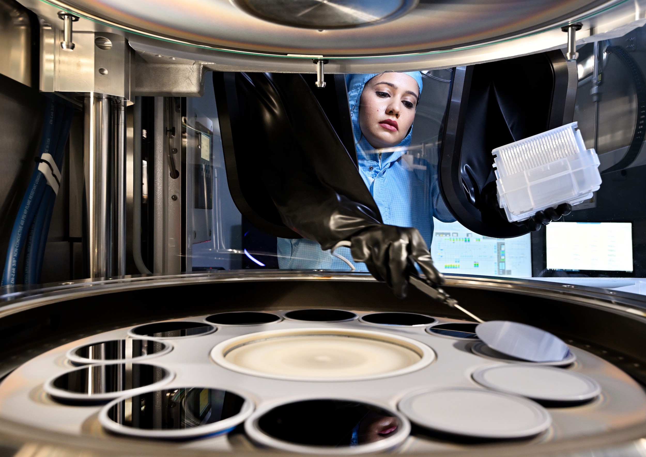
Akanksha Kapoor handling 4 inch InP wafers in the next-generation AIXTRON epitaxy reactor.
Improving hardware and experiments
Her postdoctoral project at the Electrical Engineering department is aimed at improving the epitaxy processes for the next generation of photonic integrated chips. ‘The main challenge for the coming phase is to scale up in size the rest of the line, from 3 to 4 inch wafers. We are installing and customizing tools and processes to achieve this, and at the same time experiment with the possibilities the technology has to offer. We have an active collaboration with AIXTRON, which has a lot of experience with epitaxy, but at different scales and in different materials. So, experimenting with indium phosphide at this scale is just as new and exciting as it is for us.’ At the moment, all of the equipment has been installed. ‘Now we are in the preliminary phase,’ Kapoor says. ‘So far, everything looks even better than expected.’
Though the pilot line is partially functional, it is not yet delivering its full potential, says Calzadilla. ‘We are constantly improving and expanding it, also as an integral part of the PhotonDelta Growth Fund program.’ The pilot line is aimed at research and development, and explicitly meant to serve as an open infrastructure that helps academia and industry move the state of the art of the technology, he stresses. ‘That is also where the Photonic Integration Technology Center comes in. The aim of that center is to build bridges between scientific findings and commercial applications. Through the PITC, we engage in collaborations to develop next generation manufacturing technologies, devices and circuits. We welcome any SMEs and large-scale companies who want to explore the possibilities of our InP pilot line to enable the future of integrated photonics and quantum technologies.’